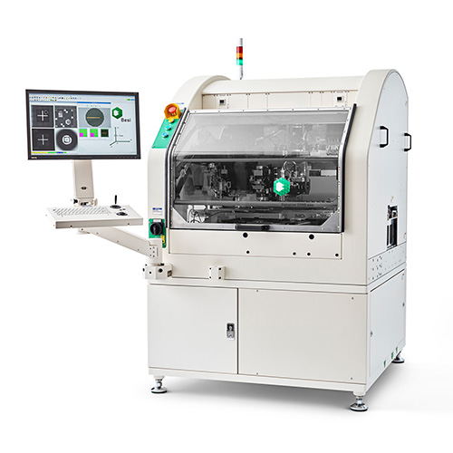
Besi Datacon 2200EVO
Key Features High Performance at High Accuracy Highest accuracy ± 10 µm @ 3 Sigma (7 µm on request) High productivity, low cost-of-ownership Up to 4 working heads in one machine Multi-Chip Cap…
Product introduction
Key Features
High Performance at High Accuracy
- Highest accuracy ± 10 µm @ 3 Sigma (7 µm on request)
- High productivity, low cost-of-ownership
- Up to 4 working heads in one machine
Multi-Chip Capability
- Single pass production for complex products
- Die attach, flip chip, multi-chip in one machine
- Epoxy writing & stamping, flux dipping
Unbeaten Flexibility
- Die pick from wafer, waffle pack, gel pack, feeder
- Die place to carrier, boat, substrate, PCB, lead frame, wafer
- Hot and cold processes supported: epoxy, soldering, thermo-compression
- MCM, SiP, Hybrids
Open Platform Architecture for Full Customization
- Most advanced modular platform concept
- Production line tailored 100% to your needs
- Ideal solution with smallest footprint possible
Specifications
Performance
- X/Y placement accuracy: ± 10 µm @ 3s
- Theta placement accuracy: ± 0.15° @ 3s
- Bond Force: 0.5N to 75N programmable
UPH
- Die attach: up to 7,000 UPH/module
- Flip Chip with dipping: up to 2,500 UPH/module
- Flip Chip without dipping: up to 3,200 UPH/module
Bond Heads
- Standard bond head 0° – 360° rotation
- Heated bond head up to 450°C (optional)
- UV Curing (365 nm & 405 nm)
Machine Dimensions
- LxDxH: 1,160 mm x 1,225 mm x 1,750 mm
- Weight: 1,300 kg
Statistics
- Uptime > 98 %
- Yield > 99.95 %
Wafer
- Die size Die Attach: 0.17 mm – 50 mm
- Die size Flip Chip: 0.5 mm – 50 mm
- Die thickness: >50 µm (thinner on request)
- Wafer size: 4″ – 12″ (SEMI M1)
- Frame size: FF070, FF105, FF108, FF123; automatic change (others on request)
Chip Trays
- Waffle pack / Gel-Pak® 2” x 2” and 4” x 4”
- JEDEC tray on request
Substrates and Carriers
- FR4, ceramic, BGA, flex, boat, lead frame, waffle pack
- Gel-Pak®, JEDEC tray, odd-shape substrates
- Substrate working range: 13” x 8” (325 mm x 200 mm)
Options
- Hardware: Open platform architecture for full customization
- Software: Single component tracking, CAD download, wafer mapping, substrate mapping, barcode scanner, datamatrix recognition and more